
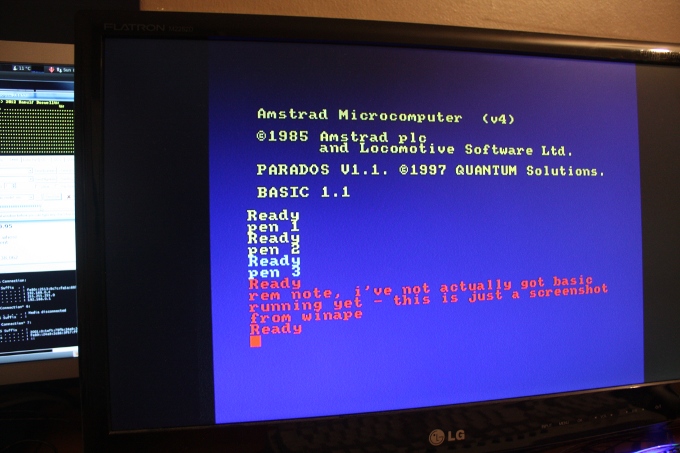
As you can see, it's pretty handy having my SREC loader as I can just load in a raw binary file to screen memory. :) There are a few things left to do with the gate array, such as the interrupt generation and ROM banking, and then to be at the basic CPC 464 state I just need to implement the AY-8912 and the PPI chip (or at least the keyboard part). I guess that means I need to dig out my soldering iron to build a PS/2 keyboard interface and level converter (the FPGA is 3.3v IO, the PS/2 port is 5v).
No comments:
Post a Comment