Monday 30 January 2012

Botched attempt at a new SCART board

I've had a pretty bad cold now for just over a week and on Saturday, rather than face the outside, I knocked together a new "SCART board" that turned into an "almost everything but the kitchen sink" board:
new board

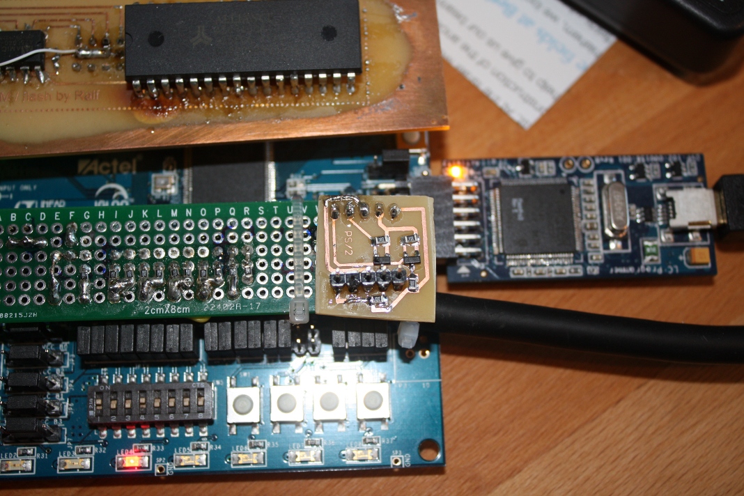
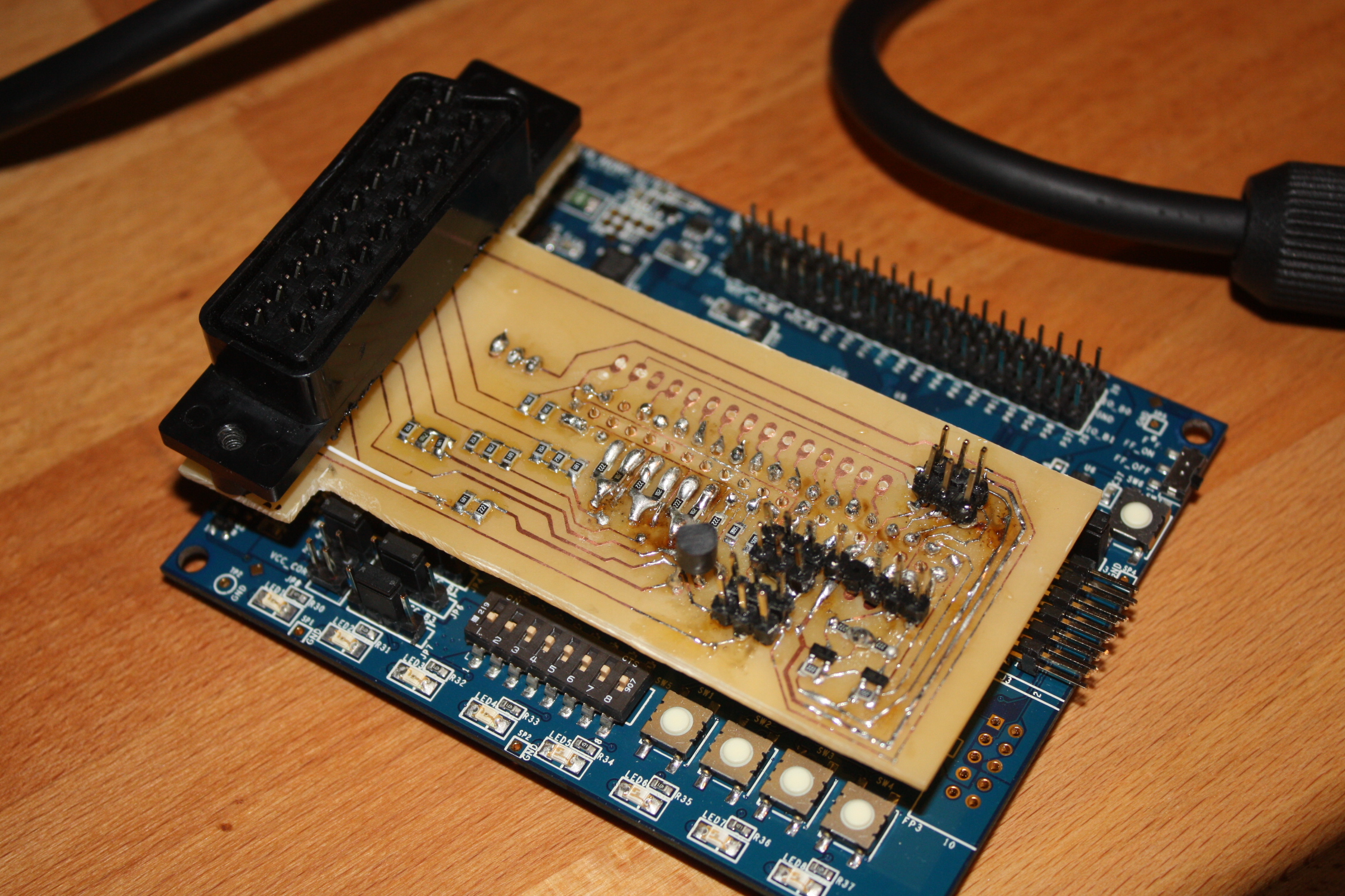
I got a bit carried away designing - I even reworked all the top half memory board too, until I discovered that whilst my DIP32 chip fitted over the 3x20 way header perfectly, the smaller SMD chips I have left would have to be placed on the board and there wasn't room to run all the traces without reordering all the pins.

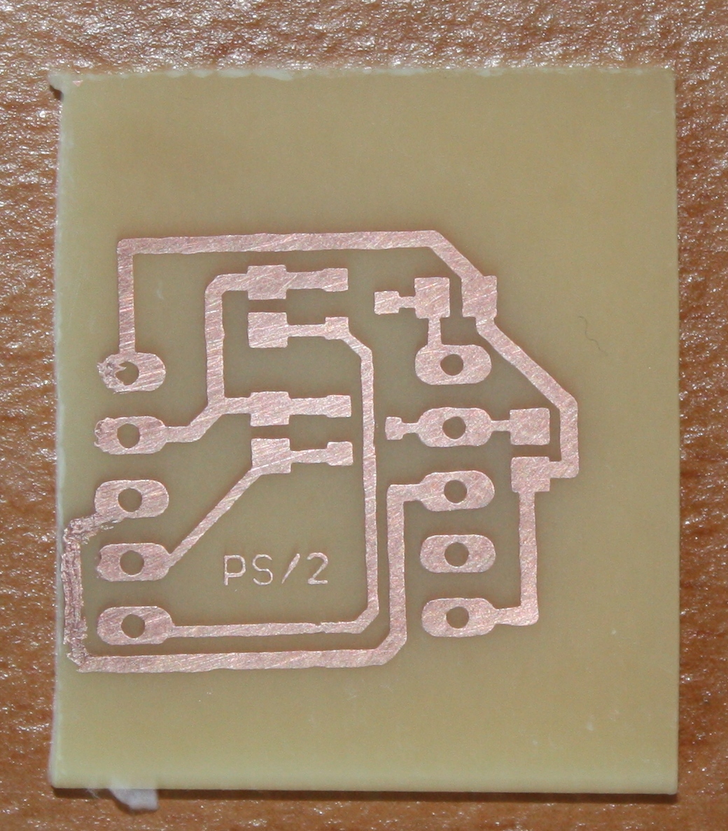
But this board did have a tape adaptor (in, out and motor), PS/2 keyboard, audio jumpers (so I could connect a speaker instead of going through SCART) and a breakout connector for the 3 buttons I'd originally designed for (which are implemented by the left 3 push switches on the mainboard). However, it looks like this board didn't really work...

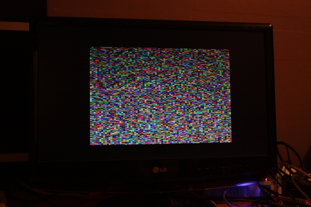
Basically, the reason for designing this board at all was that the picture from the current board didn't work too well. It's a bit shimmery and the sync seems "iffy". As in, the picture is fine for a while and then just wobbles a lot and the picture disappears. There isn't a picture at all even on my TV downstairs and the new 12" TV I bought for the FPGA was very twitchy.

Eventually, I had the bright idea of measuring the current and realised that I was drawing far too much current through the FPGA, whose pins are supposed to drive about 8mA. I was probably easily exceeding that on the sync and quite close for RGB. So, I decided I need to drive the current through transistors and as luck would have it, I found a few BC548s knocking around in my electronics tub from an IR receiver I was building years ago.

After a simple start with all the SMT components, I moved on to the headers. Soldering these on top of the board was a mess. Most of the plastic melted. I'm going to have to get some SMT ones that are designed for this. Matters weren't helped by the really small pads I'd used for the headers. I'd designed my own component based on a 20x2 way header and beefed it up to 20x3 way using a python script. This was mistake 1. The original board was done with 3 separate 1x20 way headers which leaves big pads. I'd forgotten how hard solder is to actually get to stick to thin traces. I then realised that the transistors on the underside didn't fit because of all the banks of jumpers on the FPGA board that disconnect all the LEDs and switches on the board. So, I had to desolder them and bend them to fit. This ripped up all the collector traces. HURR!

After much fiddling, I eventually patched up the board, measured all the resistances for complete traces or shorts and all was well. Plugged it in and... NOTHING. Perplexed, I plugged it into the TV in parallel via my 3 way SCART block (a bad idea, but worth it) - there were patches of colour overlaying the other picture, so something was working... but the sync was all wrong.

I decided the TV couldn't possibly be presenting 75 ohm impedance and so my voltage divider wasn't working, but this wasn't it either - I fashioned a 68 ohm resistor out of 100 and 220 through hole resistors and measured the voltage and sure enough, it was about 0.065v which was about right for the sync pulse at 16/64 duty cycle. Stumped, I prodded around the scart box and discovered that pin 20 wasn't supplying a voltage at all... But pin 19 was. Then it dawned on me. SCART leads swap a few of the connections.

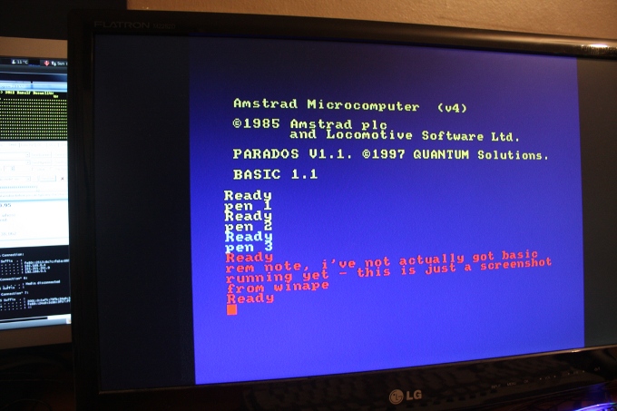
I started hacking up the composite trace with a sharp knife and then joining it up at the correct place. Plugged it in and the picture was terrible. Eventually, I got a half decent picture by applying a lateral pressure to the SCART socket, so clearly either the plug or socket isn't very high quality, but after all that work, it's not all that much better than before. Here's the test picture:
test pattern
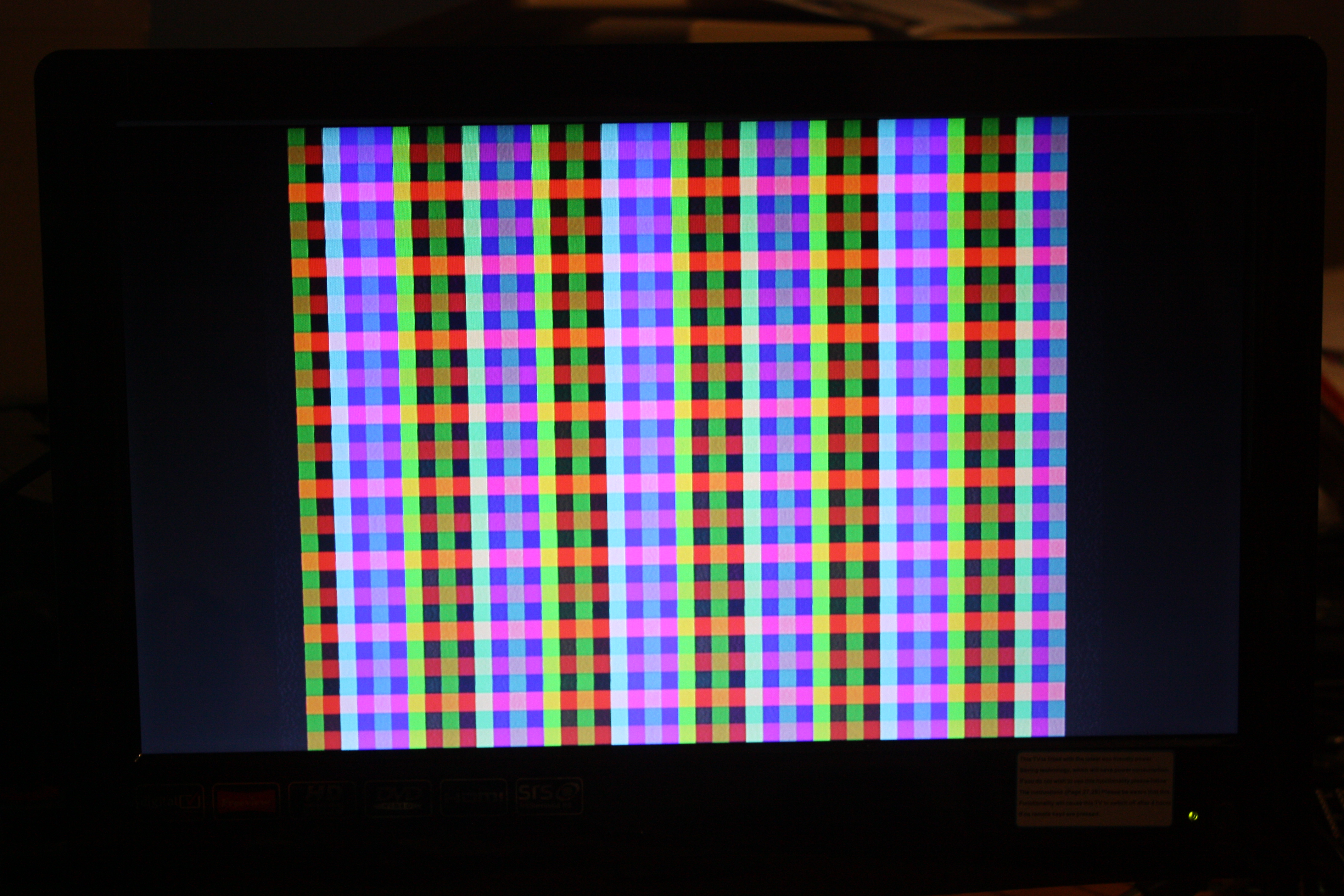
The sync is a bit more stable on the new TV, but doesn't seem to work at all on my LG. There's a slight bend at the top of the screen (although that could just be the test pattern not providing a correct sync of 5 half lines at the top of the frame) and the image still has speckles here and there. So, basically, back to the drawing board. Still, at least I've learned a few more soldering DON'Ts in this process! But seriously, SMT is so much easier, I can't wait until I'm using a custom board where I can just heat gun the whole thing!

Saturday 14 January 2012

New mystery hardware

Today, I built some new hardware... I won't tell you just yet, because I'm sure you can guess what this is going to be from the PCB. You'll also notice that I plonked the image down too close to the edge leaving a very nasty trace which I had to patch up later. When I was designing this is all looked really tiny, so I left lots of space between all the components that I certainly don't think I actually needed as the board looks very empty...
pcb ps2 keyboard adapter

If you're still guessing, here's a hint. It uses this circuit twice...

Here's a nice "arty" shot of the board, and if you haven't guessed already, you'll see the header now has a keyboard socket plugged into it (taken from an old PC which very handily just had a 5-pin header on the motherboard that this plugged into):
ps2 keyboard adapter

All in all, I'm pretty happy with this. There's a few spurious issues - on reset you quite often get a few seconds of random keypresses and occasionally key make/break scancodes are missed resulting in missed or repeated keypresses. But it's close and was pretty fun to do some soldering again!

And here's the obligatory youtube video... :)

Thursday 12 January 2012

A momentous moment...

So, I knocked up some ROM bank switching code this morning before work and only got to try it out this evening... and discovered after a few hours the simple mistake I'd introduced to keep myself on my toes... ;)

Anyway, with that in place, copying the ROM images to the flash ROM and making a bootloader to pull them in and I get this:


It's obviously pretty flakey... it worked in this shoot, but it seems to have about a 50-50 chance of actually booting and sometime between recording that video and writing this, I've noticed the cursor is no longer solid but stripey. But, this thing is so close now I can almost reach out and touch it... :)

Wednesday 11 January 2012

After a bit of tweaking, I seem to have instructions timings just about correct... I'd hyper-corrected all memory accesses meaning there was an unnecessary wait state in a normal memory read which only seemed to show up in the 4-3-5 T-state pattern used in relative jumps, so those instructions were padded out to 1us longer than on a real CPC.

Additionally, I'd been struggling with the interrupt generation for a couple of days with it resolutely refusing to work right. I tracked that down to a typo and I was resetting the counter on the 2nd pixel in a hsync rather than the 2nd hsync in a vsync... Ooops!

So, compared to WinAPE, it's almost there now...

Tomorrow I'll try to get ROM banking working at which point I might be able to get BASIC booting. At the moment, there's a single "ROM" which is used for the boot image.

Sunday 8 January 2012

gate array video output

So now I've got the video data being decoded correctly and going through the CLUT in the gate array in all 3 video modes: mode 1
mode 0
mode 2
As you can see, it's pretty handy having my SREC loader as I can just load in a raw binary file to screen memory. :) There are a few things left to do with the gate array, such as the interrupt generation and ROM banking, and then to be at the basic CPC 464 state I just need to implement the AY-8912 and the PPI chip (or at least the keyboard part). I guess that means I need to dig out my soldering iron to build a PS/2 keyboard interface and level converter (the FPGA is 3.3v IO, the PS/2 port is 5v).

Saturday 7 January 2012

SPI interface working

After much fiddling about today fighting against the VHDL compiler which was adamant that even though I'd tested my design in the simulator, it wasn't going to compile a process using both rising and falling edges of the clock. I split this up into 2 processes and all went away. The reason behind this is that with SPI, the data is always written on the rising edge and received on the falling edge...

After things returning bogus data (but always the same bogus data), I tried to debug this and realised that I was changing the sense of din and dout about 5 times between the CPU and the SPI output port, so I decided to just rename everything read and write. There obviously was a logic mistake in there, as now everything almost worked... :)

Well, not quite, but I could work around the problem:

serial output

As you can see from the line marked KLUDGE, I have to do a bogus read as the in returns the previous byte transferred not the next byte. That was a bit annoying, as I'd done my calculations and I should be able to exactly fit 8 cycles into 2 T-states, but again due to a fix I had to make to the t80 core, the out is actually only active for 1 T-state before the result is sampled... :(

Anyway, now this works, I can start uploading images to the flash memory... :)

Friday 6 January 2012

serial uart now supports receive

I added receive support to my uart yesterday morning, but spent the afternoon with family so didn't get to do much with it. I was back to work today, but this evening I've knocked up an SREC loader:


This means that if I want to experiment with Z80, I can now upload new code in a matter of seconds instead of embedding it as a fake ROM inside the FPGA which requires about 7 minutes to compile and flash.

Obviously, it's still slow to work on the hardware side of things, but this will be a massive help testing out the flash chip, as well as getting large amounts of data onto it...

Wednesday 4 January 2012

London Dungeon and outdoor skating

Yesterday, I took a day off from coding and popped down to London to catch up with my sister's family and one of my brother's daughters. We had a great day out - a trip round the London Dungeon (which I've not been to for maybe 20 years since I was the age of my nieces and nephews) and then off to Somerset House for a spot of outdoor skating.

I then caught up with a uni friend before heading back home on the train... Nice! That said, 5am-11pm is quite a long day and it took until lunch time today before I really began to feel awake!

Multiplexing video and CPU access

Of the roles the gate array performs in the CPC range, memory multiplexing is the most important. What it does is insert wait states so that the CPU only ever accesses memory 1 cycle in every 4, and using the 2 of the remaining 3 to read memory for video display.

After being plagued with subtle timing issues for a while, the view here of the simulator is left from the point when I realised my emulation of this might actually be working:

serial output

After the 7 minutes of compile time, I finally got to see it working... :)


Most of the problems were actually a complete lack of documentation for the opencores.org T80 softcore I'm using. There's a couple of parameters you specify when creating an instance and in a couple of significant areas it defaults to being almost, but slightly different to the Z80 timing diagrams...

Next up... decoding the pixel data correctly and adding the CLUT. After that, I'll work on memory banking and trying to use the flash chip.

retiring spugl domain

Well, it's time to retire the project that started this blog almost 4 years ago...

SPUGL logo

I was making fairly good progress on it, but after I started working in a games company, it took 6 months for their legal department to give me permission to continue working on my own project and by then we were deep into crunch and I really didn't want to do any hobby coding after a 10+ hour day.

Since OtherOS has been officially removed from the PS3, I've had no inclination to go back and revisit this project, even despite the unofficial ways of running linux on the PS3 now, so I think now the time is right to retire the domains. I've renewed them for a few years past working on the project, but since nobody is even looking at them it's just not worth keeping them around any longer...

I guess it was a great thing in terms of getting me a job in the games industry, it's just a shame that I felt like I was pushing the boundaries of what was possible on the PS3 in the early days before getting a job in games and since I've been in games, I've barely written any SPU code at all. Shame - it is without a doubt the nicest ISA I've even worked with...

Monday 2 January 2012

crtc working, video access kinda...

So, I've got the CRTC working. That was actually pretty painless and got it working in a couple of hours early New Year's Eve. So, that was 2 days ago. I can't have just been sat on my backside ever since! Well, apart from a nice bike ride today, I have in fact been busy.

I spent most of yesterday trying to reverse engineer what the gate array actually does to multiplex the RAM access. After a lot of time working out potential scenarios by poring over the Z80 datasheet diagrams and T-state breakdowns compared to the actual CPC instruction timings, it became apparent that it all works out pretty easy if the video uses cycles T1 and T3 (when considered as an instruction fetch) and adds a wait state after T2 in a normal read/write cycle and latching the read data even though we already have it available so we can present it at the end of T3, it all works out nicely. In fact, I'm not even sure why Amstrad also add a delay cycle to IO requests as they don't cause RAM collisions...

Anyway, with all that figured out, I started trying to implement the gate array. Getting the video memory accesses working was kind of simple, although I haven't implemented the pixel decoding yet, so instead I'm just outputting them as raw 2-bit RGB data. Actually, this mode looks kind of cool, so I might implement this as a special feature anyway:

serial output

What's a bit trickier is that I've managed to bugger up the Z80's access to memory in the process. It's close, very very close, but just after the OUT instruction the delayed refresh triggers my latch logic and I start an extra fake memory request. Actually, just describing this make me confident I've seen the problem. Tools like the VHDL simulator are awesome, though. Kids these days don't know how lucky they are! Here's the point where it all goes wrong!

serial output