Sunday, 8 January 2012

gate array video output

So now I've got the video data being decoded correctly and going through the CLUT in the gate array in all 3 video modes: mode 1
mode 0
mode 2
As you can see, it's pretty handy having my SREC loader as I can just load in a raw binary file to screen memory. :) There are a few things left to do with the gate array, such as the interrupt generation and ROM banking, and then to be at the basic CPC 464 state I just need to implement the AY-8912 and the PPI chip (or at least the keyboard part). I guess that means I need to dig out my soldering iron to build a PS/2 keyboard interface and level converter (the FPGA is 3.3v IO, the PS/2 port is 5v).

Saturday, 7 January 2012

SPI interface working

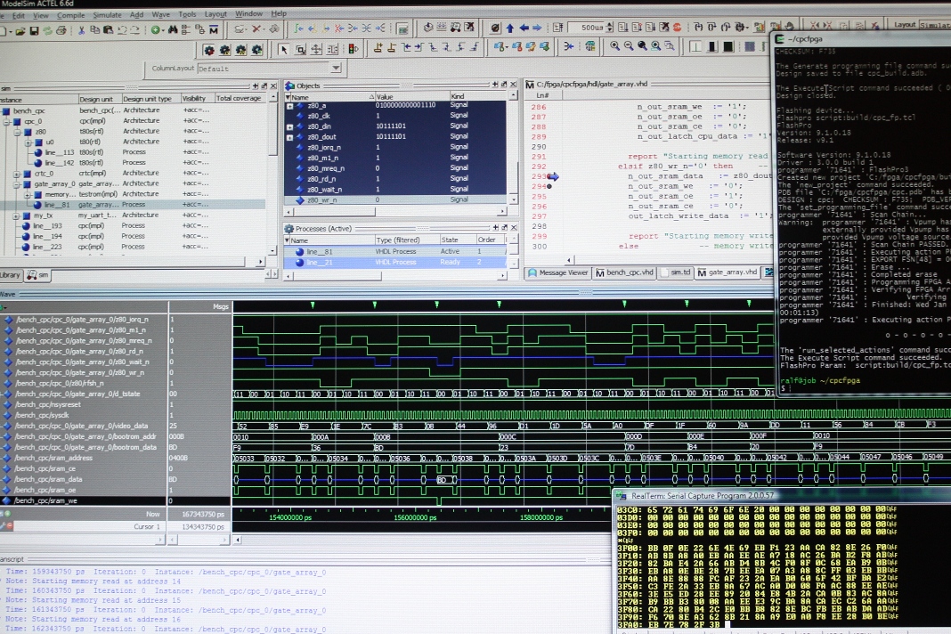
After much fiddling about today fighting against the VHDL compiler which was adamant that even though I'd tested my design in the simulator, it wasn't going to compile a process using both rising and falling edges of the clock. I split this up into 2 processes and all went away. The reason behind this is that with SPI, the data is always written on the rising edge and received on the falling edge...

After things returning bogus data (but always the same bogus data), I tried to debug this and realised that I was changing the sense of din and dout about 5 times between the CPU and the SPI output port, so I decided to just rename everything read and write. There obviously was a logic mistake in there, as now everything almost worked... :)

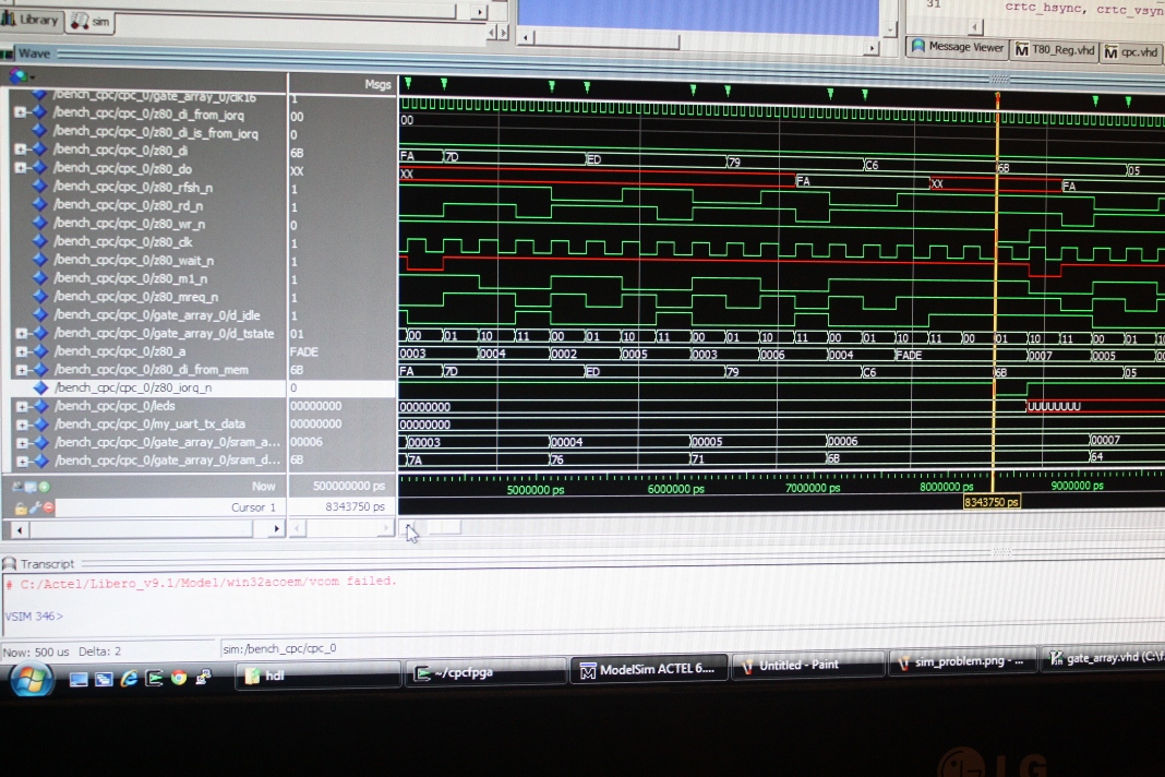
Well, not quite, but I could work around the problem:

serial output

As you can see from the line marked KLUDGE, I have to do a bogus read as the in returns the previous byte transferred not the next byte. That was a bit annoying, as I'd done my calculations and I should be able to exactly fit 8 cycles into 2 T-states, but again due to a fix I had to make to the t80 core, the out is actually only active for 1 T-state before the result is sampled... :(

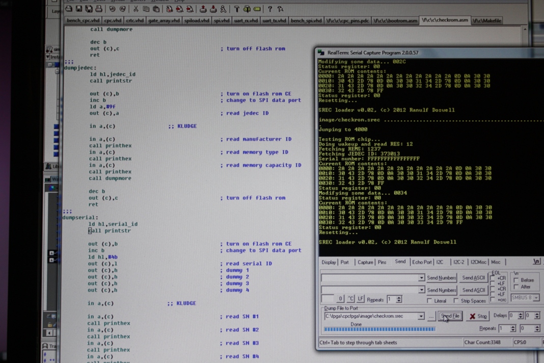
Anyway, now this works, I can start uploading images to the flash memory... :)

Friday, 6 January 2012

serial uart now supports receive

I added receive support to my uart yesterday morning, but spent the afternoon with family so didn't get to do much with it. I was back to work today, but this evening I've knocked up an SREC loader:


This means that if I want to experiment with Z80, I can now upload new code in a matter of seconds instead of embedding it as a fake ROM inside the FPGA which requires about 7 minutes to compile and flash.

Obviously, it's still slow to work on the hardware side of things, but this will be a massive help testing out the flash chip, as well as getting large amounts of data onto it...

Wednesday, 4 January 2012

London Dungeon and outdoor skating

Yesterday, I took a day off from coding and popped down to London to catch up with my sister's family and one of my brother's daughters. We had a great day out - a trip round the London Dungeon (which I've not been to for maybe 20 years since I was the age of my nieces and nephews) and then off to Somerset House for a spot of outdoor skating.

I then caught up with a uni friend before heading back home on the train... Nice! That said, 5am-11pm is quite a long day and it took until lunch time today before I really began to feel awake!

Multiplexing video and CPU access

Of the roles the gate array performs in the CPC range, memory multiplexing is the most important. What it does is insert wait states so that the CPU only ever accesses memory 1 cycle in every 4, and using the 2 of the remaining 3 to read memory for video display.

After being plagued with subtle timing issues for a while, the view here of the simulator is left from the point when I realised my emulation of this might actually be working:

serial output

After the 7 minutes of compile time, I finally got to see it working... :)


Most of the problems were actually a complete lack of documentation for the opencores.org T80 softcore I'm using. There's a couple of parameters you specify when creating an instance and in a couple of significant areas it defaults to being almost, but slightly different to the Z80 timing diagrams...

Next up... decoding the pixel data correctly and adding the CLUT. After that, I'll work on memory banking and trying to use the flash chip.

retiring spugl domain

Well, it's time to retire the project that started this blog almost 4 years ago...

SPUGL logo

I was making fairly good progress on it, but after I started working in a games company, it took 6 months for their legal department to give me permission to continue working on my own project and by then we were deep into crunch and I really didn't want to do any hobby coding after a 10+ hour day.

Since OtherOS has been officially removed from the PS3, I've had no inclination to go back and revisit this project, even despite the unofficial ways of running linux on the PS3 now, so I think now the time is right to retire the domains. I've renewed them for a few years past working on the project, but since nobody is even looking at them it's just not worth keeping them around any longer...

I guess it was a great thing in terms of getting me a job in the games industry, it's just a shame that I felt like I was pushing the boundaries of what was possible on the PS3 in the early days before getting a job in games and since I've been in games, I've barely written any SPU code at all. Shame - it is without a doubt the nicest ISA I've even worked with...

Monday, 2 January 2012

crtc working, video access kinda...

So, I've got the CRTC working. That was actually pretty painless and got it working in a couple of hours early New Year's Eve. So, that was 2 days ago. I can't have just been sat on my backside ever since! Well, apart from a nice bike ride today, I have in fact been busy.

I spent most of yesterday trying to reverse engineer what the gate array actually does to multiplex the RAM access. After a lot of time working out potential scenarios by poring over the Z80 datasheet diagrams and T-state breakdowns compared to the actual CPC instruction timings, it became apparent that it all works out pretty easy if the video uses cycles T1 and T3 (when considered as an instruction fetch) and adds a wait state after T2 in a normal read/write cycle and latching the read data even though we already have it available so we can present it at the end of T3, it all works out nicely. In fact, I'm not even sure why Amstrad also add a delay cycle to IO requests as they don't cause RAM collisions...

Anyway, with all that figured out, I started trying to implement the gate array. Getting the video memory accesses working was kind of simple, although I haven't implemented the pixel decoding yet, so instead I'm just outputting them as raw 2-bit RGB data. Actually, this mode looks kind of cool, so I might implement this as a special feature anyway:

serial output

What's a bit trickier is that I've managed to bugger up the Z80's access to memory in the process. It's close, very very close, but just after the OUT instruction the delayed refresh triggers my latch logic and I start an extra fake memory request. Actually, just describing this make me confident I've seen the problem. Tools like the VHDL simulator are awesome, though. Kids these days don't know how lucky they are! Here's the point where it all goes wrong!

serial output